


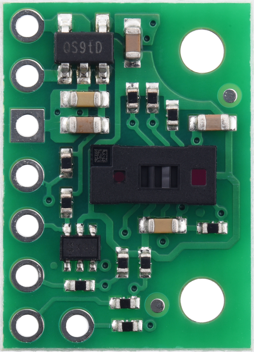
VL53L8CX Time-of-Flight 8×8-Zone Distance Sensor Carrier with Voltage Regulators, 400cm Max
Available with a lead time
Expect dispatch between Jul 27 and Jul 29
Quantity Discounts:
- 10+ $35.83 (exc GST)
- 25+ $34.71 (exc GST)
Note: This product is not recommended for use with 8-bit microcontrollers. Initializing the VL53L8CX and processing its readings require a significant amount of RAM and code space, making this sensor impractical for use with a typical 8-bit microcontroller. (ST’s API for the VL53L8CX typically uses over 90 KB of program memory.) For alternatives that are simpler to use and can work with 8-bit microcontrollers (but do not have the multi-zone or multi-target capabilities of the VL53L8CX), please consider the VL53L1X, VL53L0X carrier, or VL6180X carrier.
 |
The VL53L8CX from ST Microelectronics is a long-distance, ranging time-of-flight (TOF) sensor integrated into a compact module. This board is a carrier for the VL53L8CX, so Pololu recommend careful reading of the VL53L8CX datasheet (4MB pdf) before using this product.
The VL53L8CX is effectively a tiny, self-contained lidar system featuring an integrated 940 nm Class 1 laser, which is invisible and eye-safe. Unlike conventional IR sensors that use the intensity of reflected light to estimate the distance to an object, the VL53L8CX uses ST’s FlightSense technology to precisely measure how long it takes for emitted pulses of infrared laser light to reach the objects and be reflected back to a detector. This approach ensures absolute distance measurements independent of ambient lighting conditions and target characteristics (e.g. color, shape, texture, and reflectivity), though these external conditions do affect the maximum range of the sensor.
The VL53L8CX is distinguished from ST’s more basic time-of-flight sensors by its multi-zone ranging output: its field of view is divided into a number of zones, configurable as a 4×4 or 8×8 grid, and the sensor provides separate readings for each zone (which can include multiple targets per zone). This effectively makes the VL53L8CX a basic 3D lidar, since instead of measuring only a single distance (1D lidar), it can provide enough data to generate a low-resolution depth map of the environment within its field of view. The following image shows an example of such a map made with the VL53L5CX, which is similar to the VL53L8CX:
 |
A plot of a coffee cup as detected by a VL53L5CX time-of-flight 8×8-zone distance sensor. |
|---|
Under favorable conditions, the VL53L8CX can report distances up to 4 m (13 ft) with 1 mm resolution. This sensor has the same maximum range as the older VL53L5CX, as the 4 m specification assumes an ideal dark environment, but the VL53L8CX performs better in situations with higher ambient light. For example, in 5000 lux of ambient light (medium to bright indirect sunlight), the VL53L8CX can be expected to see a large reflective target up to 2.8 m (9.2 ft) away, compared to about 1.7 m (5.6 ft) for the VL53L5CX. The minimum ranging distance is 20 mm.
The sensor can be configured and its ranging measurements can be accessed through a digital interface, which can be configured to operate in either I²C (TWI) mode at up to 1 MHz or SPI mode at up to 3 MHz. (Note: In Pololu's experience, the SPI frequency must be higher than about 1.1 MHz or problems with initializing the sensor can result.) The sensor also provides additional pins that include an interrupt output and an external synchronization input.
The VL53L8CX is a great IC, but its small, leadless, LGA package makes it difficult for the typical student or hobbyist to use. It also requires multiple voltage supplies and uses a 1.8 V maximum logic voltage, which can make interfacing difficult for microcontrollers operating at 5 V or 3.3 V. Pololu's breakout board addresses these issues, making it easier to get started using the sensor, while keeping the overall size as small as possible.
The carrier board includes two voltage regulators that provide the 1.8 V and 3.3 V required by the VL53L8CX and allows the sensor to be powered from a single 3.2 V to 5.5 V supply. The regulator outputs are available on the CORE/IOVDD (1.8 V) and AVDD (3.3 V) pins and can supply around 50 mA and 200 mA, respectively, to external devices. The breakout board also includes a level shifter that shifts all of the VL53L8CX’s I/O lines to the same logic voltage level as the supplied VIN, making it simple to interface the board with 5 V and 3.3 V systems. The board ships fully populated with its SMD components, including the VL53L8CX, as shown in the product picture.
The pins are spaced to work with standard 0.1" (2.54 mm) male headers and 0.1" female headers (available separately), making the board easy to use with solderless breadboards and 0.1" perfboards. The board has two mounting holes that work with #2 and M2 screws (not included).
 |
VL53L8CX Time-of-Flight 8×8-Zone Distance Sensor Carrier on a breadboard. |
|---|
Alternative versions
The VL53L8CX is essentially an upgraded version of the VL53L5CX, with the same multi-zone capability and FoV, but the VL53L8CX has better performance in ambient light and support for SPI communication at up to 3 MHz (which can significantly speed up initialization and data acquisition). The VL53L7CX is also similar but has a wider FoV and a slightly shorter range.
Pololu's VL53L8CX carrier board is larger than Pololu's VL53L5CX and VL53L7CX boards, but the power and I²C pins are arranged the same way, so this VL53L8CX board can be used as a pin-compatible replacement in many applications. Additionally, the VL53L8CX API is very similar to the VL53L5CX/VL53L7CX API, so it is generally possible to upgrade to the VL53L8CX with minimal software changes. For other related sensors, see the comparison section at the bottom of this page.
|
|

Features and specifications
- Dimensions: 0.5" × 0.9" × 0.1" (13 mm × 23 mm × 3 mm)
- Weight without header pins: 0.7 g (0.03 oz)
- Operating voltage: 3.2 V to 5.5 V
- Typical active-ranging supply current: 100 mA
- Varies with configuration, target, and environment; peak current can reach 150 mA
- Maximum range: 4 m (13 ft)
- Resolution: 1 mm depth, 4×4 or 8×8 sensor zones
- Minimum range: 20 mm (0.8 in)
- Emitter: 940 nm invisible Class 1 VCSEL (vertical cavity surface-emitting laser) – eye-safe
- Detector: SPAD (single photon avalanche diode) receiving array
- Typical full field of view (FoV): 65° diagonal (45° horizontal/vertical)
- Output format (I²C/SPI): histogram
Using the VL53L8CX
Important note: This product might ship with a protective liner covering the sensor IC. The liner must be removed for proper sensing performance.
 |
Connections
 |
| Pin | Description |
|---|---|
| CORE/IOVDD | Regulated 1.8 V output. Up to around 50 mA is available to power external components. |
| AVDD | Regulated 3.3 V output. Up to around 200 mA is available to power external components. (Note that a VIN voltage lower than about 3.4 V will cause the AVDD to drop below the nominal 3.3 V; however, the VL53L8CX accepts an AVDD voltage as low as 3.13 V.) |
| VIN | This is the main 3.2 V to 5.5 V power supply connection. The level shifter shifts all I/O lines to this level (and pulls them high by default). |
| GND | The ground (0 V) connection for your power supply. Your I²C or SPI control source must also share a common ground with this board. |
| SDA/MOSI | Level-shifted I²C data line and SPI data in line. |
| SCL/MCLK | Level-shifted I²C/SPI clock line. |
| MISO | Level-shifted SPI data out line. |
| CS | Level-shifted SPI enable (chip select); active low. Pulled high by default; a falling edge is required to start SPI communication. (This pin is called NCS in the datasheet.) |
| INT | Level-shifted programmable interrupt output. |
| SPI/I2C | Level-shifted SPI/I²C mode select pin. Pulled high by default, selecting SPI mode; drive low to select I²C mode (can also be toggled to reset I²C interface). (This pin is called SPI_I2C_N in the datasheet.) |
| LP | Level-shifted I²C disable input (active low). Pulled high by default; driving this pin low disables I²C communication (typically used as part of a process to change I²C addresses). (This pin is called LPn in the datasheet.) |
| SYNC | Level-shifted external synchronization pin. The VL53L8CX can be configured to have a rising edge on this pin trigger a single ranging acquisition. |
Regardless of the interface being used to communicate with the VL53L8CX, its VIN pin should be connected to a 3.2 V to 5.5 V source, and GND should be connected to 0 volts.
A minimum of two logic connections is necessary to use the VL53L8CX in I²C mode: SCL and SDA. These pins are connected to an on-board level shifter that makes them safe to use at voltages above the VL53L8CX’s 1.8 V logic voltage; they should be connected to an I²C bus operating at the same logic level as VIN. Additionally, the SPI/I2C pin must be driven low to select I²C communication; a convenient way to do this is by connecting it to the adjacent GND pin (e.g. with a pair of header pins and a shorting block).
To use the VL53L8CX in SPI mode, four logic connections are typically used: MCLK, MOSI, MISO, and CS. These level-shifted pins should be connected to an SPI bus operating at the same logic level as VIN.
The INT, LP, and SYNC pins are additional I/O pins that enable more advanced functionality. The board’s level shifter pulls up all of the I/O pins on the VL53L8CX by default.
Note: The level shifter on the VL53L8CX carrier board is more sensitive to external loads than the circuit Pololu use for level shifting on most of Pololu's other I²C boards. Therefore, you should take extra care to keep connected communication wires short (ideally under 3 inches or 8 cm) and limit other devices on the same I²C or SPI bus.
In certain situations, adding a small amount of capacitance (a few tens of picofarads) to the interface lines can help prevent undesired signal oscillations caused by the level shifter; however, too much capacitance can slow down communication speeds or cause other issues.
Schematic diagram
 |
The above schematic shows the additional components the carrier board incorporates to make the VL53L8CX easier to use, including the voltage regulators that allows the board to be powered from a 3.2 V to 5.5 V supply and the level shifter circuit that allows for I²C and SPI communication at the same logic voltage level as VIN. This schematic is also available as a downloadable PDF (107k pdf).
I²C communication
With the SPI/I2C pin low, the VL53L8CX can be configured and its distance readings can be queried through the I²C bus. Level shifters on the I²C clock (SCL) and data (SDA) lines enable I²C communication with microcontrollers operating at the same voltage as VIN (3.2 V to 5.5 V). A detailed explanation of the I²C interface on the VL53L8CX can be found in its datasheet (4MB pdf), and more detailed information about I²C in general can be found in NXP’s I²C-bus specification (1MB pdf).
The sensor’s 7-bit target address defaults to 0101001b on power-up. It can be changed to another value by writing one of the device configuration registers, but the new address only applies until the sensor is reset or powered off. ST’s UM3109 (1MB pdf) document describes how to use multiple VL53L8CX sensors on the same I²C bus by individually enabling I²C communication on each sensor with its LP pin and assigning it a unique address.
The I²C interface on the VL53L8CX is compliant with the I²C fast mode plus (1 MHz) standard.
SPI communication
With the SPI/I2C pin in its default state (pulled high), the VL53L8CX can be used in SPI mode. The CS pin (which is pulled high by default) must be driven low before the start of an SPI command and allowed to return high after the end of the command. Level shifters on the SPI clock (MCLK), data in (MOSI), and data out (MOSI) lines enable SPI communication with microcontrollers operating at the same voltage as VIN (3.2 V to 5.5 V). A detailed explanation of the SPI interface on the LPS22DF can be found in its datasheet (4MB pdf).
Sensor configuration and control
In contrast with the information available for many other devices, ST has not publicly released a register map and descriptions or other documentation about configuring and controlling the VL53L8CX. Instead, communication with the sensor is intended to be done through ST’s VL53L8CX ULD API (STSW-IMG040), a set of C functions that take care of the low-level interfacing. To use the VL53L8CX, you can customize the API to run on a host platform of your choice using the information in the API documentation. Alternatively, it is possible to use the API source code as a guide for your own implementation.
Pololu’s family of carriers for ST time-of-flight distance sensors
Pololu make pin-compatible carriers/breakout boards for several different ST time-of-flight (ToF) ranging sensors, as shown in the table below. They all function as tiny lidar systems featuring an integrated 940 nm Class 1 (i.e. invisible and eye-safe) laser, and they are all based on the same FlightSense technology, which precisely measures how long it takes for emitted pulses of infrared laser light to reach the objects and be reflected back to a detector. This approach ensures absolute distance measurements independent of ambient lighting conditions and target characteristics (e.g. color, shape, texture, and reflectivity), though these external conditions do affect the maximum range of the sensor. These sensors are all capable of 1 mm resolution, with some limitations on some versions.
 VL6180X carrier |  VL53L4CD carrier |  VL53L0X carrier |  VL53L1X carrier |  VL53L3CX carrier |  VL53L5CX carrier |  VL53L7CX carrier |  VL53L8CX carrier | |
|---|---|---|---|---|---|---|---|---|
| Maximum range:(1) | 60 cm | 120 cm | 200 cm | 400 cm | 500 cm | 400 cm | 350 cm | 400 cm |
| Minimum range: | ~10 mm | 1 mm | ~30 mm | 40 mm | 10 mm | 20 mm | ||
| Field of view: | 25° | 18° | 25° | 15° to 27° diagonal, programmable | 25° | 65° diagonal, up to 8×8 zones | 90° diagonal, up to 8×8 zones | 65° diagonal, up to 8×8 zones |
| Other features: | ambient light sensing, low memory footprint(2) | low memory footprint(2), ultra-low power mode | low memory footprint(2) | low memory footprint(2), ultra-low power mode | multi-target detection, ultra-low power mode | multi-target detection | multi-target detection | multi-target detection, improved performance in ambient light |
| Maximum update rate:(1) | ~150 Hz | 100 Hz | 50 Hz | 100 Hz | 125 Hz | 60 Hz | ||
| Operating voltage range: | 2.6 V to 5.5 V | 2.5 V to 5.5 V | 3.2 V to 5.5 V | |||||
| Regulator voltage: | 2.8 V | 3.3 V | 1.8 V and 3.3 V | |||||
| Typical active-ranging supply current: | 25 mA | 25 mA | 20 mA | 20 mA | 20 mA | 100 mA | ||
| Peak supply current: | 40 mA | 150 mA | ||||||
| Interface: | I²C | I²C, SPI | ||||||
| Dimensions: | 0.5" × 0.7" | 0.5" × 0.9" | ||||||
| 1 Effective range and update rate depend on configuration, target, and environment. 2 Suitable for use with typical 8-bit MCUs. | ||||||||
Most of these carriers have the same physical dimensions (0.5" × 0.7") and work in 3.3 – 5 V systems (thanks to their integrated linear regulators and level-shifters), and they can all be controlled through an I²C interface. However, they have different APIs and memory requirements, so software will generally need to be rewritten when switching between sensors in an application, and versions with higher memory requirements are generally not suitable for use with typical 8-bit microcontrollers.
People often buy this product together with:
 | VL53L7CX Time-of-Flight 8×8-Zone Wide FOV Distance Sensor Carrier with Voltage Regulator, 350cm Max |
Dimensions
| Size: | 0.5" × 0.9" × 0.1" |
|---|---|
| Weight: | 0.7 g |
General specifications
| Resolution: | 1 mm |
|---|---|
| Maximum range: | 400 cm1 |
| Minimum range: | 2 cm |
| Interface: | I²C, SPI |
| Minimum operating voltage: | 3.2 V |
| Maximum operating voltage: | 5.5 V |
| Supply current: | 100 mA2 |
Identifying markings
| PCB dev codes: | irs19b |
|---|---|
| Other markings: | 0J14398 |
Notes:
- 1
- Effective range depends on configuration, target, and environment.
- 2
- Typical active-ranging supply current; varies with configuration, target, and environment. Peak current can reach 150 mA.
File downloads
-
VL53L8CX datasheet (4MB pdf)
-
This DXF drawing shows the locations of all of the board’s holes.
-
UM10204 I²C-bus specification and user manual (1MB pdf)
The official specification for the I²C-bus, which is maintained by NXP.
Recommended links
-
ST’s product page for the VL53L8CX time-of-flight multizone ranging sensor IC, with links to its most up-to-date datasheet, software, and other resources.
-
VL53L8CX ULD API (STSW-IMG040)
ST’s Ultra Lite Driver API (application programming interface) for the VL53L8CX.
Exact shipping can be calculated on the view cart page (no login required).
Products that weigh more than 0.5 KG may cost more than what's shown (for example, test equipment, machines, >500mL liquids, etc).
We deliver Australia-wide with these options (depends on the final destination - you can get a quote on the view cart page):
- $3+ for Stamped Mail (typically 10+ business days, not tracked, only available on selected small items)
- $7+ for Standard Post (typically 6+ business days, tracked)
- $11+ for Express Post (typically 2+ business days, tracked)
- Pickup - Free! Only available to customers who live in the Newcastle region (must order online and only pickup after we email to notify you the order is ready). Orders placed after 2PM may not be ready until the following business day.
Non-metro addresses in WA, NT, SA & TAS can take 2+ days in addition to the above information.
Some batteries (such as LiPo) can't be shipped by Air. During checkout, Express Post and International Methods will not be an option if you have that type of battery in your shopping cart.
International Orders - the following rates are for New Zealand and will vary for other countries:
- $12+ for Pack and Track (3+ days, tracked)
- $16+ for Express International (2-5 days, tracked)
If you order lots of gear, the postage amount will increase based on the weight of your order.
Our physical address (here's a PDF which includes other key business details):
40 Aruma Place
Cardiff
NSW, 2285
Australia
Take a look at our customer service page if you have other questions such as "do we do purchase orders" (yes!) or "are prices GST inclusive" (yes they are!). We're here to help - get in touch with us to talk shop.
Have a product question? We're here to help!
 VL53L5CX 8x8 Time of Flight (ToF) Array Sensor BreakoutSKU: PIM622 Brand: PimoroniA sophisticated distance sensor with 8x8 multizone ranging and a wide field of v ...
- SparkFun Distance Sensor Breakout - 4 Meter, VL53L1X (Qwiic)SKU: SEN-14722 Brand: SparkfunThis SparkFun Distance Sensor Breakout utilizes the VL53L1X next generation ToF ...
- Adafruit MCP2221A Breakout - General Purpose USB to GPIO ADC I2C - Stemma QT / QwiicSKU: ADA4471 Brand: AdafruitWouldn't it be cool to drive a tiny OLED display, read a color sensor, or even j ...
- VL53L0X Time-of-Flight Distance Sensor Carrier with Voltage Regulator, 200cm MaxSKU: POLOLU-2490 Brand: PololuThis sensor is a carrier/breakout board for ST’s VL53L0X laser-ranging sensor, ...


- PiicoDev Cable Expansion KitSKU: CE09146 Brand: PiicoDev
Top up your PiicoDev Starter kit with a range of the most used cables!
- MPU-6050 Module 3 Axis Gyroscope + AccelerometerSKU: 018-MPU-6050 Brand: Core ElectronicsA 3-axis gyroscope and 3-axis accelerometer housed on a development board ready ...
- HC-SR04 Ultrasonic Module Distance Measuring SensorSKU: CE05112 Brand: Core ElectronicsThe HC-SR04 ultrasonic sensor uses sonar to determine distance to an object like ...
- Jumper Wire 20cm Ribbon (F/F, 40pcs)SKU: CE05098 Brand: Core ElectronicsJumpstart your electronics project with a pack of 40, 20cm female-to-female jump ...
Videos
View AllGuides

Effective Ways To Measure Distance In Maker Projects

DIY 2D and 3D Spatial Tracking with Ultra-Wideband | Arduino & Pico Guide

Getting Started With Ultra-Wideband & Measuring Distances| Arduino & Pico Guide

The Maker Revolution
Projects

WhyzaGC - Feather ESP32 addon to the MightyOhm Gieger Counter

IR Break-Beam Stopwatch

Makers love reviews as much as you do, please follow this link to review the products you have purchased.
Product Comments