Logic Level Shifter, 4-Channel, Bidirectional
In stock, ships same business day if ordered before 2PM
Delivered by Tue, 5th of May
Quantity Discounts:
- 10+ $5.15 (exc GST)
- 25+ $4.99 (exc GST)
 |
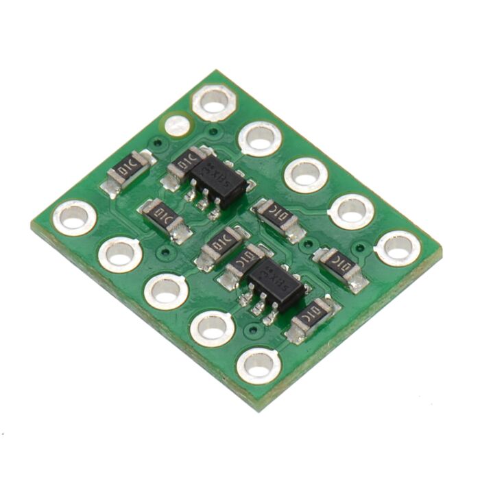
As digital devices get smaller and faster, once ubiquitous 5 V logic has given way to ever lower-voltage standards like 3.3 V, 2.5 V, and even 1.8 V, leading to an ecosystem of components that need a little help talking to each other. For example, a 5 V part might fail to read a 3.3 V signal as high, and a 3.3 V part might be damaged by a 5 V signal. This level shifter solves these problems by offering bidirectional voltage translation of up to four independent signals, converting between logic levels as low as 1.5 V on the lower-voltage side and as high as 18 V on the higher-voltage side, and its compact size and breadboard-compatible pin spacing make it easy to integrate into projects.
The logic high levels on each side of the shifter are achieved by 10 kO pull-up resistors to their respective supplies; these provide quick enough rise times to allow decent conversion of fast mode (400 kHz) I²C signals or other similarly fast digital interfaces (e.g. SPI or asynchronous TTL serial). External pull-ups can be added to speed up the rise time further at the expense of higher current draw. See the schematic diagram below for more information.
Features
- Dual-supply bus translation:
- Lower-voltage (LV) supply can be 1.5 V to 7 V
- Higher-voltage (HV) supply can be LV to 18 V
- Four bidirectional channels
- Small size: 0.4" × 0.5" × 0.08" (13 mm × 10 mm × 2 mm)
- Breadboard-compatible pin spacing
Connections
 |
Example wiring diagram for connecting 5 V and 3.3 V devices through the 4-channel bidirectional logic level shifter. |
|---|
This logic level converter requires two supply voltages: the lower-voltage logic supply (1.5 V to 7 V) connects to the LV pin and the higher-voltage supply (LV to 18 V) connects to the HV pin. The HV supply must be higher than the LV supply for proper operation. Logic low voltages will pass directly from Hx to the corresponding Lx (and vice versa), while logic high voltages will be converted between the HV level to the LV level as the signal passes from Hx to Lx or Lx to Hx.
The level shifter circuit does not require a ground connection to either device, so there are no ground pins on the board. (Some competing level shifter modules provide ground connections that simply act as a pass-through; Pololu have opted to leave these off and make the board smaller.) The two devices being connected through the level shifter must still share a common ground.
The picture below shows a level-shifted TTL serial connection (RX and TX) between a 5 V Arduino Uno and a 3.3 V Raspberry Pi.
 |
Using the 4-channel bidirectional logic level shifter to create a serial connection between a 5 V Arduino Uno and a 3.3 V Raspberry Pi. |
|---|
Included hardware
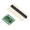
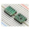
A 0.1"-pitch male header strip is included for use with this board. The strip can be broken into smaller pieces and soldered in so the board can be used with perfboards, breadboards, or 0.1" female connectors. Alternatively, wires can be soldered directly to the board for more compact installations. The connections are labeled on the back side of the of the PCB, so you might find it more convenient to solder the pins in the way that allows the labeled side to be facing up.
|
|
Schematic diagram
The logic level conversion is accomplished with a simple circuit consisting of a single n-channel MOSFET and a pair of 10 kO pull-up resistors for each channel. When Lx is driven low, the MOSFET turns on and the zero passes through to Hx. When Hx is driven low, Lx is also driven low through the MOSFET’s body diode, at which point the MOSFET turns on. In all other cases, both Lx and Hx are pulled high to their respective logic supply voltages. External pull-ups can be added to speed up the rise time. This same circuit is detailed in NXP’s application note on I²C bus level-shifting techniques (54k pdf), and Pololu have used it before on carrier boards for 3.3 V sensors with I²C interfaces – like the MinIMU-9 – to enable them to work directly with both 3.3 V and 5 V systems.
 |
This schematic is also available as a downloadable PDF (135k pdf).
People often buy this product together with:
 | 0.1" (2.54mm) Crimp Connector Housing: 1x2-Pin 25-Pack |
 | 0.1" (2.54mm) Crimp Connector Housing: 1x4-Pin 10-Pack |
 | Female Crimp Pins for 0.1" Housings 100-Pack |
Dimensions
| Size: | 0.4" × 0.5" × 0.08"1 |
|---|---|
| Weight: | 0.3 g1 |
Identifying markings
| PCB dev codes: | ls01a |
|---|---|
| Other PCB markings: | 0J8121 |
Notes:
File downloads
-
Logic Level Shifter schematic diagram (135k pdf)
Printable schematic diagram of the Logic Level Shifter, 4-Channel, Bidirectional.
-
Logic Level Shifter dimension drawing (81k pdf)
Detailed dimension drawing of the Logic Level Shifter, 4-Channel, Bidirectional.
-
3D model of the Logic Level Shifter (2MB step)
-
Level shifting techniques in I2C-bus design (54k pdf)
Application note by NXP describing bidirection level shifting techniques for Fast-mode and Standard-mode I2C-bus systems.
Exact shipping can be calculated on the view cart page (no login required).
Products that weigh more than 0.5 KG may cost more than what's shown (for example, test equipment, machines, >500mL liquids, etc).
We deliver Australia-wide with these options (depends on the final destination - you can get a quote on the view cart page):
- $3+ for Stamped Mail (typically 10+ business days, not tracked, only available on selected small items)
- $7+ for Standard Post (typically 6+ business days, tracked)
- $11+ for Express Post (typically 2+ business days, tracked)
- Pickup - Free! Only available to customers who live in the Newcastle region (must order online and only pickup after we email to notify you the order is ready). Orders placed after 2PM may not be ready until the following business day.
Non-metro addresses in WA, NT, SA & TAS can take 2+ days in addition to the above information.
Some batteries (such as LiPo) can't be shipped by Air. During checkout, Express Post and International Methods will not be an option if you have that type of battery in your shopping cart.
International Orders - the following rates are for New Zealand and will vary for other countries:
- $12+ for Pack and Track (3+ days, tracked)
- $16+ for Express International (2-5 days, tracked)
If you order lots of gear, the postage amount will increase based on the weight of your order.
Our physical address (here's a PDF which includes other key business details):
40 Aruma Place
Cardiff
NSW, 2285
Australia
Take a look at our customer service page if you have other questions such as "do we do purchase orders" (yes!) or "are prices GST inclusive" (yes they are!). We're here to help - get in touch with us to talk shop.
Have a product question? We're here to help!
Guides
The Maker Revolution
Projects
Raspberry Pi Cyberdeck (SDR Edition)
Pico-Dog Motion Activated Audio Alarm
WaveJumper: Music Sample Slicer on a Breadboard
Makers love reviews as much as you do, please follow this link to review the products you have purchased.





Product Comments