Dual MC33926 Motor Driver Carrier
Available with a lead time
Expect dispatch between Apr 29 and May 04
Quantity Discounts:
- 6+ $62.18 (exc GST)
- 12+ $60.24 (exc GST)
January 2022 availability update: This product has been affected by the global parts shortages, and Pololu do not know when Pololu will be able to make more, so Pololu are not accepting backorders at this time. As an alternative, Pololu recommend Pololu's TB9051FTG carriers, which offer very similar performance. They are available as a single carrier or as a dual motor driver shield for arduino (which can also be used as a dual carrier).
Overview
 |
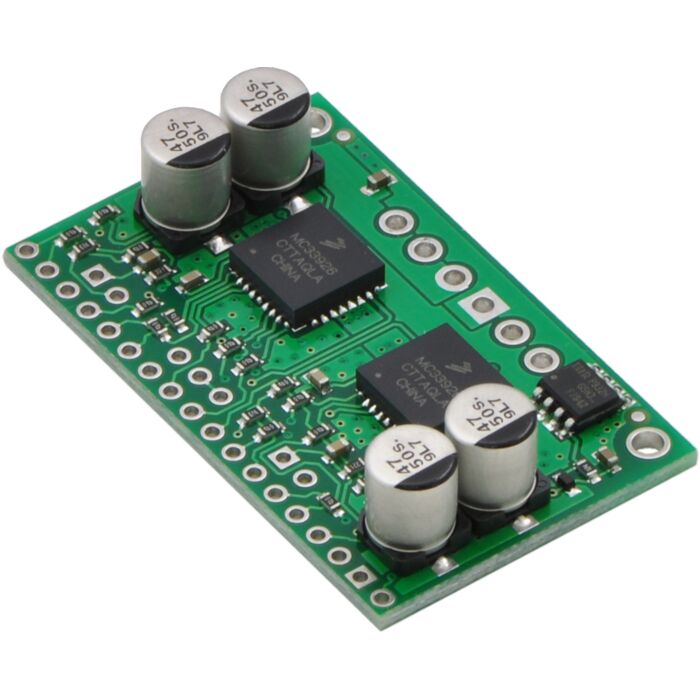
The dual MC33926 motor driver carrier is a breakout board featuring two Freescale MC33926 H-bridge ICs. It can supply up to almost 3 A continuous current per channel to two brushed DC motors at 5 V to 28 V, and it can tolerate peak currents up to 5 A per channel for a few seconds, making this a great general-purpose motor driver for medium-sized DC motors and for differential-drive robots that use such motors. The MC33926 supports ultrasonic (up to 20 kHz) pulse width modulation (PWM) of the motor output voltage, which eliminates the audible switching sounds caused by PWM speed control, and a current feedback circuit for each motor outputs an analog voltage on its respective FB pin that is proportional to the output current. Since this board is a carrier for the Freescale Semiconductor MC33926 H-bridge, Pololu recommend careful reading of the MC33926 datasheet (1MB pdf).
For a single-driver version of this board, please consider the MC33926 motor driver carrier.
Pinout
 |
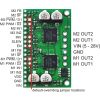
The default states of many of the MC33926 logic input pins requires that many external connections be made to use this board. To reduce the number of necessary external connections, the board has seven default-overriding jumpers. All of the default-overriding jumpers are tied to VDD, except the D1 jumpers, which are tied to GND. All VDD jumper pads are circles; the ground jumper pads are square. Note that the board has only one invert, slew, and enable pin; each of these three pins affects both motor drivers.
| PIN | Default State | Description |
|---|---|---|
| VIN | HIGH | This is the main 5 V to 28 V motor power supply connection, which should typically be made to the larger VIN pad. Operation from 5 V to 8 V reduces maximum current output; the device is also protected for transients up to 40 V. The smaller VIN pad can be used to distribute the VIN node to the rest of the application circuit; for lower-current applications, the pin can also be used to power the board and motors. |
| GND | LOW | Ground connection for logic and motor power supplies. |
| OUT2 | HIGH | The motor output pin controlled by IN2. |
| OUT1 | HIGH | The motor output pin controlled by IN1. |
| VDD | HIGH | 3 V to 5 V logic supply connection. This pin is used only for the SF pull-up and default-overriding jumpers; in the rare case where none of those features is used, VDD can be left disconnected. |
| IN2 | HIGH | The logic input control of OUT2. PWM can be applied to this pin (typically done with both disable lines inactive). |
| IN1 | HIGH | The logic input control of OUT1. PWM can be applied to this pin (typically done with both disable lines inactive). |
| PWM / D2 | LOW | Inverted disable input: when D2 is low, OUT1 and OUT2 are set to high impedance. A D2 PWM duty cycle of 70% gives a motor duty cycle of 70%. Typically, only one of the two disable pins is used, but the default is for both disable pins to be active. |
| PWM / D1 | HIGH | Disable input: when D1 is high, OUT1 and OUT2 are set to high impedance. A D1 PWM duty cycle of 70% gives a motor duty cycle of 30%. Typically, only one of the two disable pins is used, but the default is for both disable pins to be active. |
| SF | HIGH | Status flag output: an over-current (short circuit) or over-temperature event will cause SF to be latched LOW. If either of the disable pins (D1 or D2) are disabling the outputs, SF will also be LOW. Otherwise, this pin is weakly pulled high. This allows the two SF pins on the board to be tied together and connected to a single MCU input. |
| FB | LOW | The FB output provides analog current-sense feedback of approximately 525 mV per amp (only active while H-bridge is driving). |
| EN | LOW | Enable input: when EN is LOW, the both motor driver ICs are in a low-current sleep mode. |
| SLEW | LOW | Output slew rate selection input. A logical LOW results in a slow output rise time (1.5 µs to 6 µs). A logical HIGH selects a fast output rise time (0.2 µs to 1.45 µs). This pin should be set HIGH for high-frequency (over 10 kHz) PWM. This pin determines the slew rate mode for both motor driver ICs. |
| INV | LOW | A logical high value inverts the meaning of IN1 and IN2 for both motor drivers. |
Basic Application Connections
In a typical application, five I/O lines are used to connect each motor driver channel to a microcontroller: the two input lines, IN1 and IN2, for direction control, one of the disable lines, D1 or D2, for PWM speed control, the current sense output, FB, for monitoring motor current draw (connected to an analog-to-digital converter input) and the status flag, SF, for monitoring motor driver errors. The control lines can be reduced to two pins per channel if PWM signals are applied directly to the two input pins with both disable pins held inactive. In each of these cases, the other unused lines must be set to enable proper operation. For example, if D2 is used for the PWM input (as is typically the case), D1 must be held low to prevent it from disabling the motor driver. The circuit board provides convenient jumper points for overriding the motor driver defaults without having to connect extra wires to the module.
The current sense and status flag connections are optional, though monitoring of the status flags can allow detection of latched fault conditions. The status flags are open-drain output, so the two status flag can be wired together for applications where I/O pins are scarce and determining which motor driver is experiencing a fault condition is not necessary.
Note that the default state of the enable pin, EN, is LOW, which holds both motor driver chips in a low-current sleep mode. You will need to hold this pin high (either with an external connection or via the default-overriding jumper next to the pin) to allow the board to run.
Protection
The MC33926 has under-voltage, over-current, and over-temperature protection. Some protection events are indicated by the status flag pins (SF).which are active-low pins that can be connected connected to a single input. If the chip detects an over-current or over-termperature event, the SF is latched LOW and OUT1 and OUT2 are set to high-impedance. To unlatch the status flag pin toggle the D1, D2 , EN or VIN lines. The carrier board has a reverse-protection MOSFET for added protection to the motor driver chips.
Current sensing
The current sense output is approximately 525 mV/A. Note that the output is only active while the corresponding H-bridge is driving; it is inactive (low) when the driver is braking or the motor outputs are high impedance (floating). If the driver is braking, current will continue to circulate through the motor, but the voltage on the FB pin will not accurately reflect the motor current. Please note that like most motor drivers with integrated current sense, the actual sensitivity can vary significantly from unit to unit, and accuracy is derated for currents below 0.5 A (see the MC33926 datasheet (1MB pdf) for more information). Please consider Pololu's Hall effect current sensors as options for adding more consistent and accurate current sensing to your system.
Real-World Power Dissipation Considerations
The MC33926 motor driver used on this carrier board has a maximum current rating of 5 A continuous. However, the chip by itself will overheat at lower currents. For example, in Pololu's tests at room temperature with no forced air flow, the chip was able to deliver 5 A for 5 s and 4 A for 18 s before the chip’s thermal protection started reducing the current. A continuous current of 3 A was right at the over-temperature threshold; in some tests the thermal protection kicked in after a minute, and in other tests the chip delivered 3 A for over five minutes without triggering thermal protection. The actual current you can deliver will depend on how well you can keep the motor driver cool. The carrier’s printed circuit board is designed to draw heat out of the motor driver chips, but performance can be improved by adding a heat sink. Pololu's tests were conducted at 100% duty cycle; PWMing the motor will introduce additional heating proportional to the frequency.
This product can get hot enough to burn you long before the chip overheats. Take care when handling this product and other components connected to it.
Unlike other H-Bridges, the 33926 has a feature that allows it to gracefully reduce current as the current exceeds 5 A or as the chip temperature approaches its limit. This means that if you push the chip close to its limit, you will see less power to the motor, but it might allow you to avoid a complete shutdown.
Included Hardware
|
|
A 25-pin straight breakaway male header is included with the MC33926 dual carrier board, which can be used to connect the PCB to perfboards or breadboards. The board also includes three 2-pin 3.5mm terminal blocks for making simple motor connections.
Schematic Diagram
 |
People often buy this product together with:
 | TB6612FNG Dual Motor Driver Carrier |
 | Pololu Universal Aluminum Mounting Hub for 6mm Shaft, #4-40 Holes (2-Pack) |
 | Pololu Stamped Aluminum L-Bracket Pair for 37D mm Metal Gearmotors |
Dimensions
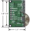
| Size: | 1.10" x 1.8"1 |
|---|---|
| Weight: | 0.25 oz |
General specifications
| Motor driver: | MC33926 |
|---|---|
| Motor channels: | 2 |
| Minimum operating voltage: | 5 V2 |
| Maximum operating voltage: | 28 V3 |
| Continuous output current per channel: | 2.5 A4 |
| Current sense: | 0.525 V/A |
| Maximum PWM frequency: | 20 kHz5 |
| Minimum logic voltage: | 2.5 V |
| Maximum logic voltage: | 5.5 V |
| Reverse voltage protection?: | Y6 |
Notes:
- 1
- Without included hardware
- 2
- Operation from 5 V to 8 V reduces maximum current output.
- 3
- The device is protected for transients up to 40 V.
- 4
- Can be improved by addition of heat sink or forced air flow.
- 5
- SLEW pin should be HIGH for frequencies above 10 kHz.
- 6
- On motor voltage only; logic voltage does not have reverse protection.
File downloads
-
MC33926 H-Bridge Datasheet (1MB pdf)
The datasheet for Freescale’s MC33926 H-bridge.
-
Dimension diagram of the Dual MC33926 Motor Driver Carrier (249k pdf)
-
3D model of the Dual MC33926 Motor Driver Carrier (5MB step)
Note: this model applies to boards manufactured after December 2014; before this, the electrolytic capacitors were 0.07" taller, making the total height 0.37".
-
Dual MC33926 Motor Driver Carrier drill guide (99k dxf)
This DXF drawing shows the locations of all of the board’s holes.
Exact shipping can be calculated on the view cart page (no login required).
Products that weigh more than 0.5 KG may cost more than what's shown (for example, test equipment, machines, >500mL liquids, etc).
We deliver Australia-wide with these options (depends on the final destination - you can get a quote on the view cart page):
- $3+ for Stamped Mail (typically 10+ business days, not tracked, only available on selected small items)
- $7+ for Standard Post (typically 6+ business days, tracked)
- $11+ for Express Post (typically 2+ business days, tracked)
- Pickup - Free! Only available to customers who live in the Newcastle region (must order online and only pickup after we email to notify you the order is ready). Orders placed after 2PM may not be ready until the following business day.
Non-metro addresses in WA, NT, SA & TAS can take 2+ days in addition to the above information.
Some batteries (such as LiPo) can't be shipped by Air. During checkout, Express Post and International Methods will not be an option if you have that type of battery in your shopping cart.
International Orders - the following rates are for New Zealand and will vary for other countries:
- $12+ for Pack and Track (3+ days, tracked)
- $16+ for Express International (2-5 days, tracked)
If you order lots of gear, the postage amount will increase based on the weight of your order.
Our physical address (here's a PDF which includes other key business details):
40 Aruma Place
Cardiff
NSW, 2285
Australia
Take a look at our customer service page if you have other questions such as "do we do purchase orders" (yes!) or "are prices GST inclusive" (yes they are!). We're here to help - get in touch with us to talk shop.
Have a product question? We're here to help!
Guides
The Maker Revolution
Projects
Raspberry Pi Cyberdeck (SDR Edition)
Pico-Dog Motion Activated Audio Alarm
WaveJumper: Music Sample Slicer on a Breadboard
Makers love reviews as much as you do, please follow this link to review the products you have purchased.






Product Comments