When it comes to assembling a prototype Printed Circuit Board (PCB), there are a couple of options for applying solder-paste:
- Paste each individual pad by hand with a syringe, or;
- Use a stencil to paste all pads in one pass.
The first option is quite labour-intensive but extremely accessible for the average maker: great for low-quantity prototyping with minimal cost and tooling. The second option - stencilling paste onto a PCB - is truly a level-up if you have access to tools to make one. Stencils are fast and repeatable which is great for more complex PCBs or larger scale production. They're also very fast to fabricate, taking a fraction of the time it takes to mill or etch a prototype PCB. To make a stencil does require special tooling: in this case a laser-cutter. In this article I'll share the steps I took in making my first solder stencil based on our own product called GlowBit™ rainbow (GlowBit™ is our coined tradename for products we design based on WS2812 V5 LEDs) and some lessons learned along the way. This article will focus on solder stencil fabrication only - I'll assume you already have a PCB design that you're ready to prototype.
Contents
- Materials, Tools, Software
- Procedure
- Step 1: Generate Paste-Layer artwork
- Step 2: Shrink the Apertures
- Step 3: Create a material profile
- Step 4: Laser-cutting
- Conclusion
Materials, Tools, Software
For reference, I'm using:
- Stencil material - polyimide film, non-adhesive, 0.05mm thick. There isn't a very maker-friendly supply of this in Australia - we're working on it! Check back soon.
- Laser - Trotec Speedy 400 Laser Cutter with 80W CO2 laser (Not 60W, as I repeatedly say in the video).
- PCB software - KiCad which is free and open-source. It should be very straightforward to adapt the following steps to your PCB software of choice.
- Vector editing software - Adobe Illustrator. Any decent editor will do, I'll include alternate instructions for Inkscape which is free and open-source.
- Isopropyl Alcohol - for cleaning the stencil.
- Adhesive tape - secures the film to the laser bed, and is useful during stencilling.
Procedure
Step 1: PCB Software | Generate Paste-Layer artwork
The Paste Layer of a PCB design contains the apertures (holes) for the solder stencil. Find your software's export utility and export the appropriate Paste-layer as a vector image (.SVG file).
In KiCad, the steps are:
- Open the Plot dialogue
- Select the Plot format: SVG
- Deselect the unnecessary layers. Here I'm making a stencil just for the Front Paste layer (F.Paste) so it is the only Included layer
- Plot the file
The KiCad Plot dialogue for generating fabrication outputs - usually Gerber files. Here we export the Front-Paste layer as a vector image (SVG) for "printing" with a laser-cutter.
Step 2: Vector Editing Software | Shrink the apertures
Usually, the stencil apertures are the same dimensions as their corresponding pads. This is fine for PCBs that have a solder-mask layer. Since I'm working with a bare copper-clad prototype, I decided to give myself some clearance. This additional step will help prevent unwanted solder bridges forming between pads/traces and builds in a little tolerance for error in stencil-alignment. Since the laser beam has some width, this step also takes care of the kerf.
For Adobe Illustrator:
- Open the SVG file we created in Step 1
- Select the artwork and Ungroup repeatedly until you are left with only individual objects. (Object > Ungroup)
- With all the artwork selected, open the Object > Transform > Transform Each dialogue
- Apply a scale factor to shrink the apertures. I chose 80% for both Horizontal and Vertical scale
Shrink the aperture-size using a vector editing program. It's important to apply the scaling to each object independently rather than scaling the group as a whole, which would change the aperture locations.
For Inkscape, the process is very similar. The Transform dialogue contains an option to Apply to each object separately.
Step 3: Laser-Cutting | Create a material profile
Our laser-cutter works like a plotter-printer. Similarly to how a printer needs print-media settings (eg. thickness, ink/toner settings) our laser cutter requires power and speed settings for each material. Since I've never cut 0.05mm polyimide film before, I first had to create a material profile. After some research into laser-cutting PCB stencils, the consensus seems to be to use the laser's engraving function - where it rasters back and forth like a print head. The alternative would be to use the cutting function, where the laser would trace the outline of each aperture - this apparently produces inferior results, likely due to creating intense localised heat.
My process for finding Power/Speed settings:
- Set power and speed to produce a conservatively low amount of heat (low power for a given speed)
- Attempt a cut and observe results
- Increment power and repeat 2-3 until a reliable cut is achieved.
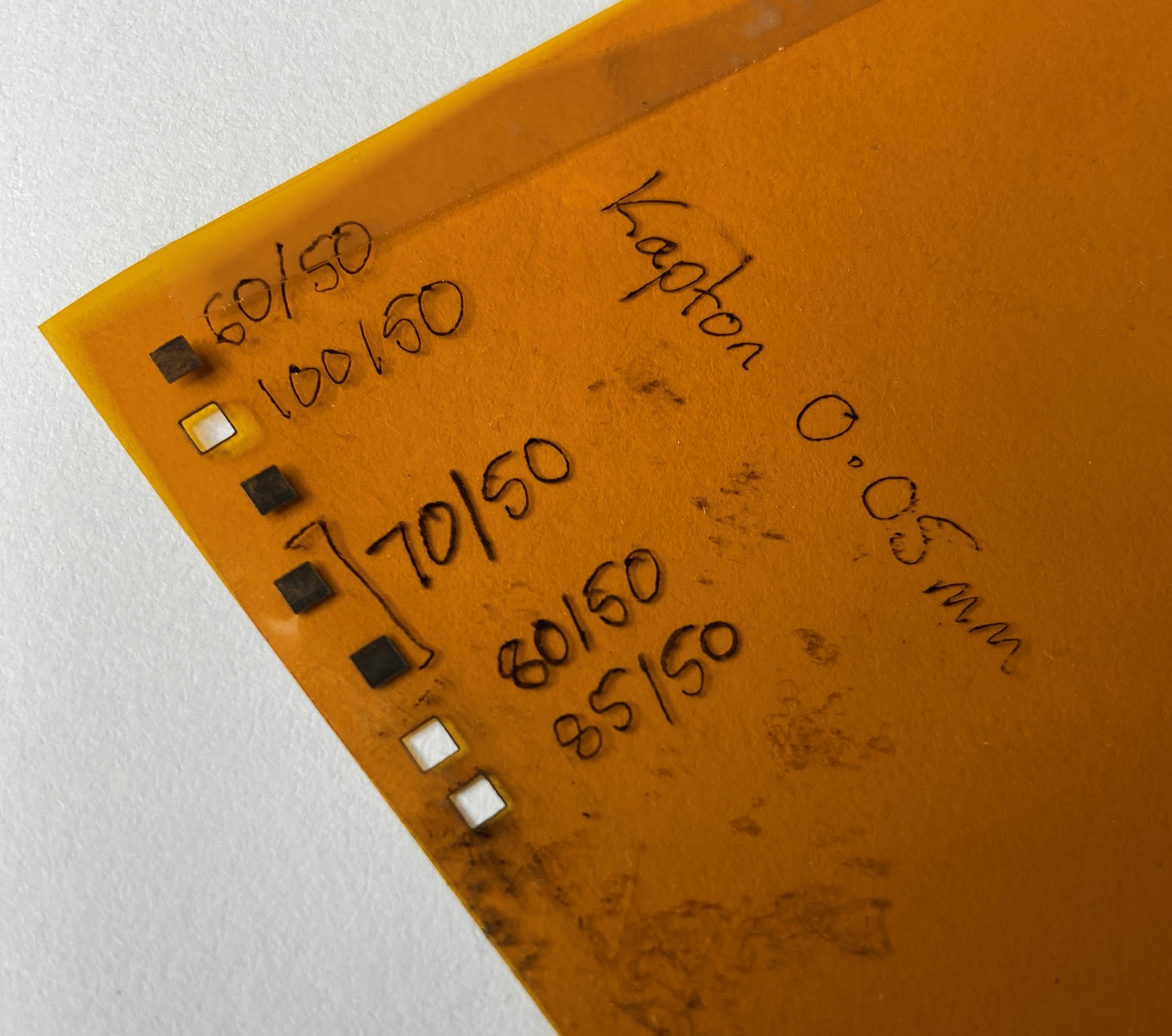
Working with this method, I found a solution that worked for my 0.05mm polyimide film on a Trotec Speedy 400 (80W CO2): 85% Power, 50% Speed. Refer to the below image for the full story.

Dialling in the Power/Speed settings on a Trotec Speedy 400: Starting with reasonably conservative power (60/50, the material only blackened), going way over-the-top (100/50) and then finding a sweet spot for reliable cutting without excessive power (85/50).
Here, I'm searching along one axis only (power). Of course, you could table-out all plausible power/speed settings in eg. 10% increments and exhaustively search the operational envelope to optimise for speed and power. Perhaps there is a more accurate, effective or faster solution available. For my design which uses 5050-package LEDs this profile worked well enough. It will be interesting to see how this profile handles smaller devices.
Step 4: Laser-Cutting | Fabricate and use the stencil
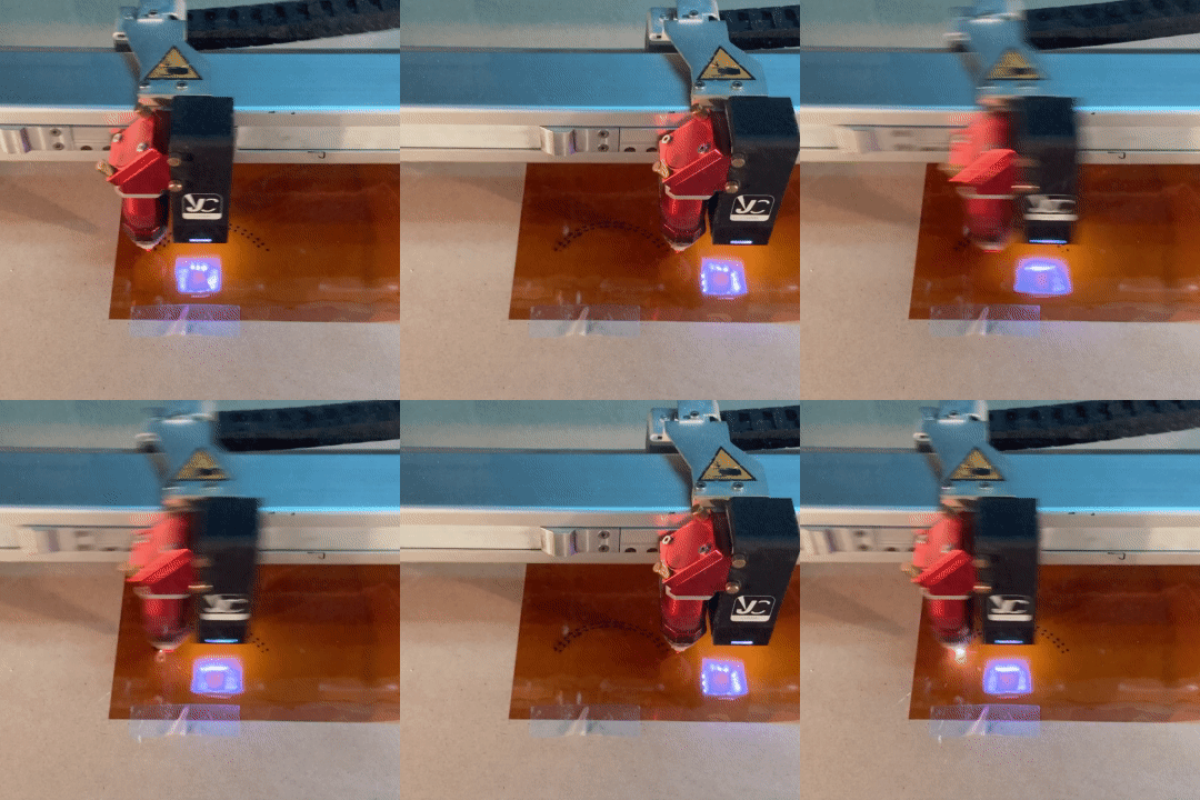
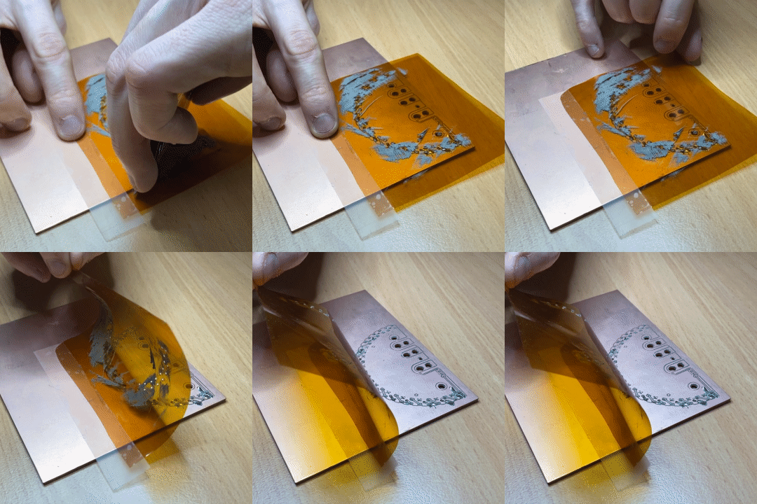
Tape the film down on some waste-material and "print" the stencil artwork. Once the stencil is cut, all that remains is to use it! This is a one-off prototype so I taped the stencil directly to the PCB. For reusability, I've seen these kinds of stencils taped to the workbench instead - the tape acts as a hinge, allowing the board to slide in and out.
 |
 |
Footnote: I'm working with Chip Quik SAC305 paste here, though I'm interested in experimenting with temperature-stable lead-free solder paste (composition: Sn42/Bi57.6/Ag0.4). If any readers have experience with the quirks of this formula I'd love to hear about it! From what I gather, the paste containing Bismuth is active at significantly lower temperatures.
Conclusion
What a level-up! Cutting your own PCB stencil may feel like a lot of set-up, but the whole process is actually very time-efficient. Now that I have a usable material profile, the whole stencil fabrication process - from generating artwork and scaling apertures, to cutting - takes about 10 minutes. That's quite a competitive timeframe versus manually dispensing solder-paste! The outcome is a reusable stencil that ought to last at least a dozen applications if treated carefully.
There's definitely some room for improvement! If you expect to be using a stencil for some small-scale manufacture, consider cutting a rigid frame with the outline of your board and glueing the stencil in place: MDF seems like a promising candidate for a cheap and easy-to-cut material. A jig/frame combo would allow repeatable, reliable stencil alignment and probably helps your stencil last longer.
If you have any tips to share we'd love to hear them! In particular, I noticed some scorching around the apertures after laser cutting - no big deal to clean with alcohol but perhaps there's some room for improvement. I'm quite happy with this first-time result and look forward to really dialling-in the process.
Framed stencils (follow-up)
I gave it a go! Here's a framed stencil I made for a really tiny board. Some parts in this design are 0402 - about the size of a grain of sand! Since this prototype has a solder-mask layer, I skipped the aperture-shrinking step. The frame is MDF which is very inexpensive, cuts well, but produces quite unpleasant fumes - ensure adequate ventillation. The PCB sits in a slot carved out by a special "material removal" profile I created - essentially a very aggressive engraving.


