 SPI stands for Serial Peripheral Interface and it is a way to send data between microcontrollers and other small devices. It is a synchronous data bus, meaning it uses a clock to regulate the data transfer.
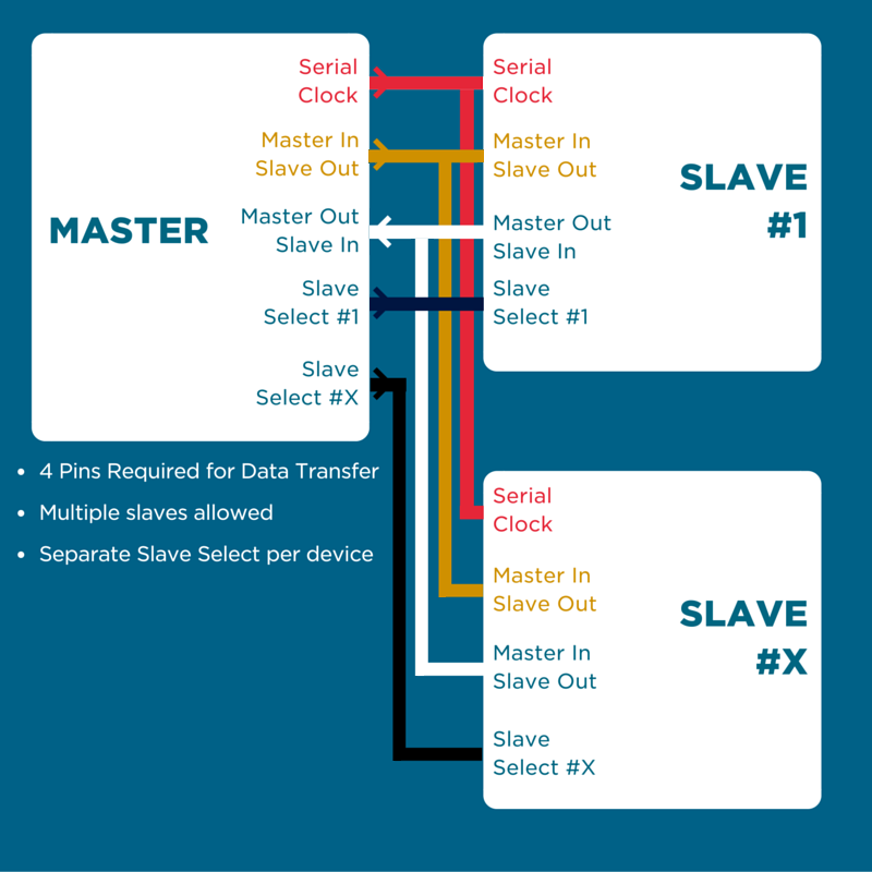
SPI is also Full-Duplex communication meaning we can have data being sent and received simultaneously.
The SPI Master is the one that generates the clock (in our case this will be the Arduino). The SPI restricts us to having 1 Master and multiple slaves, meaning the master controls communication for all the slaves. There are 4 data lines that SPI uses:
- When the Master sends data to the Slave it uses a MOSI (Master out Slave In) Line
- When the Slave wants to send data back to the Master it uses a MISO (Master in Slave Out) Line
- These 2 lines are regulated by the SCK, which is Serial Clock.
- SS Line is the slave select line. It is held high by the master until it has data to be sent. In which case, the Master drops this line low. We call this Active Low logic as the line goes low causing the slave to become active. This is sometimes referred to as an Enable line.
|
Mode |
Clock Polarity |
Clock Phase |
|
SPI_Mode0 |
0 |
0 |
|
SPI_Mode1 |
0 |
1 |
|
SPI_Mode2 |
1 |
0 |
|
SPI_Mode3 |
1 |
1 |
The clock logic regulates the sending of data and it can be configured in 4 possible modes (see table). Clock polarity refers to the logic at which the clock is set when no data is being transferred. The Clock phase represents whether the data will be read by the devices on the rising or falling edges of the clock pulses. We can also arrange the master to send additional clock signals, allowing the slave to return data in the same transfer.
The data transfer sequence (For default active low slave configuration, using default clock phase):
-
SS goes low
-
Clock toggles on
-
Master and slave each sample (read) the first bit when the clock rises the first time (unless you are using falling logic of course)
-
As the clock falls, they each prepare for the next bit
-
Step 3 and 4 are repeated until all data has been transferred.
-
When data transfer is complete, SS is set to high by the master, which switches it off.
The slave datasheet will help us identify how we should sample the clock for our data transfer.
Theoretically, we can connect one master to many slaves by connecting each slave to a separate slave select line (I/O pin on our Arduino). We can also daisy chain slave devices which will all share the same slave select, but each slave in the chain will act as the master for the following slave. The Return data must then flow through each link in the chain, resulting in massive data chunks.
Why would we use SPI?
- Some devices only support SPI.
- SPI is the fastest communication method available on the Atmega328 chip at a crazy 888,888 bytes per second (868KB/s).
- You can do both SPI and I2C simultaneously with ATmega328
|
Advantages of SPI |
Disadvantages of SPI |
|
Faster than asynchronous |
The master device controls everything |
|
Can utilize simple shift registers |
Requires 4 wires minimum, going up the more slaves you have. |
|
Supports multiple slave |
You need to have well-defined parameters for sending and receiving data |
The Project
We are going to use the Serial Peripheral Interface to communicate with a simple Shift Register to control 8 LEDs using the 4 data lines discussed above.
Components required:
- 1 x Arduino Uno board
- 1 x Solderless breadboard
- 1 x 74HC595 Shift Register
- 15 x Jumper wires
- 8 x LEDs
- 8 x 220 Ω Resistor
Software Required:
- SPI.h Library
- Arduino IDE
The Shift Register,
entering the world of integrated circuits.
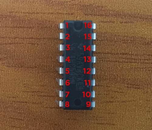
The shift register we will be using is the 74HC595N. It is a 16 pin, Serial-In-Parallel-out integrated circuit. This means the package itself has 16 pins and takes a serial input of data, breaks it down and outputs it to multiple pins. We will be using it to control 8 different LEDs using only the SPI pins from our Arduino. The shift register will be our slave device with the Arduino being the Master.
Aside: An integrated circuit is a packaged circuit that comes as a prebuilt circuit that we can interface with to fill a purpose. There are dozens of types of ICs available to consumers, today, however, we will start off using a Shift Register that is a DIP (Dual In-Line Package). Meaning the physical package has 2 parallel rows of pins.
|
The 74HC595 Shift Register |
|||
|
Pin |
Purpose |
Name |
Arduino Pin |
|
1 |
Data Out Bit 1 |
Q1 |
|
|
2 |
Data Out Bit 2 |
Q2 |
|
|
3 |
Data Out Bit 3 |
Q3 |
|
|
4 |
Data Out Bit 4 |
Q4 |
|
|
5 |
Data Out Bit 5 |
Q5 |
|
|
6 |
Data Out Bit 6 |
Q6 |
|
|
7 |
Data Out Bit 7 |
Q7 |
|
|
8 |
Ground |
GND |
|
|
9 |
Serial Data Out |
Q7S |
|
|
10 |
Master Reset (Active Low) |
MR |
|
|
11 |
Shift Register Clock Input |
SHCP |
13 |
|
12 |
Storage Register Clock Input |
STCP |
10 |
|
13 |
Output Enable (Active Low) |
OE |
|
|
14 |
Serial Data Input |
DS |
11 |
|
15 |
Data Out Bit 0 |
Q0 |
|
|
16 |
Supply Voltage |
VCC |
|
 The Setup
 The Setup
- Connect your shift register to the center of your breadboard over the vertical break, orient the chip such that Pin 1 is at the top left and Pin 16 is at the top right.
- Connect your 8 LEDs and resistors in series on separate lines.
- Connect 5v and GND from the Arduino to the breadboard as shown. This will make connecting the shift register much easier.
- Connect the Shift register to the Arduino according to both the sketch (left) and the table above.
- Use a jumper to connect pin 8 and 13 of the shift register to GND rails. Pin 8 is ground for the Shift Register and Pin 13 is the output enable pin. By connecting pin 13 to ground we are able to use the register as an output device without coding for it
- Use a jumper to connect pin 16 and 10 to the 5v rail. Pin 16 is Vcc for the shift register and pin 10 is the active low Master Reset pin, so tying it to Vcc means we will never reset the transfer.
- Finally, starting with pin 15, then pins 1-7 connect the LED array in the way shown.
Coding our SPI example
#include <SPI.h>

/*Define the pins we are using on the Arduino Board and
  cross reference them with the pins on the Shift register
  so you can give them appropriate names*/
int latchpin = 10;
int datapin = 11;
int clockpin = 13;

//Define a Variable to use for the data we are going to send,
byte data = 0;


void setup() {

  SPI.begin();                              //Start the SPI library
  SPI.setBitOrder(LSBFIRST);                //Set LSB as bit order, this means we will send the least significant bit first and it will be written to Q7 = Register Pin 7 with the most significant bit being written last to Q0 or Pin 15
  /*Configure the Arduino pins we use as OUTPUT, so they can send
     data to the Shift Register
  */
  pinMode(latchpin, OUTPUT);
  pinMode(datapin, OUTPUT);
  pinMode(clockpin, OUTPUT);

  delay(500);
}

void loop() {
  for (data = 0; data < 256; data  )        //For loop to set data = 0 then increase it by one for every iteration of the loop, when the counter reaches the condition (256) it will be reset
  {
    digitalWrite(latchpin, LOW);            //Write our Slave select low to enable the SHift register to begin listening for data
    SPI.transfer(data);                     //Transfer the 8-bit value of data to shift register, remembering that the least significant bit goes first
    digitalWrite(latchpin, HIGH);           //Once the transfer is complete, set the latch back to high to stop the shift register listening for data
    delay(500);                             //Delay program for 500ms
  }

}
Upload the code to your board, if you want a more thorough understanding of the coding process read through the comments within the code.
What you should be seeing is the LEDs blinking in a somewhat strange sequence. What’s happening here is that the Arduino is sending a number to the Shift Register over SPI.
The process we are seeing:
- The Arduino sets the slave select line low (pin 10), this lets the shift register know that data is coming.
- The shift register then prepares to read each bit by synchronizing with the clock signal on Arduino Pin 13.
- The first time this happens in our code the Arduino sends the 8 bit binary value for 0 serially to the shift register. This is 00000000.
- The right-most zero in that sequence is known as the least significant bit, which is set in a storage register inside our shift register.
- The shift register loads each bit from the Arduino one at a time into the storage register.
- The Arduino, having finished sending the value of data, sets the latch back to High.
- The storage register then sends that 8-bit sequence out in parallel to the 8 LEDs we have connected to it.
- The Arduino then adds 1 to the value of the data sent and the process is repeated until that value is 256, then the value for data is reset to 0 and the loop begins again.
Congratulations, you just got a run-down on SPI communications with the Arduino. If you have any questions or queries, don't hesistate to get in touch with us via the forum and ask!

