![]() Welcome to part 1 of our Cadsoft Eagle tutorial. Put your hand up if you’ve always wanted to take the clunky, delicate circuit you’ve created on a breadboard, and turn it into a beautifully laid out PCB (Printed Circuit Board)? Or convert that tangle of wires into a readable schematic that is easy to document and understand? If your hand is raised, then you’ve come to the right place.
Welcome to part 1 of our Cadsoft Eagle tutorial. Put your hand up if you’ve always wanted to take the clunky, delicate circuit you’ve created on a breadboard, and turn it into a beautifully laid out PCB (Printed Circuit Board)? Or convert that tangle of wires into a readable schematic that is easy to document and understand? If your hand is raised, then you’ve come to the right place.
Today we’re going to look at how to use the wildly popular Cadsoft Eagle designed software to turn any DIY project into a professional PCB. This tutorial will be broken up into 3 separate articles. We’ll start by learning how to create a schematic that will translate well into a PCB layout, then we’ll look at creating a PCB layout and what to aim for/avoid, and finally we’ll finish off with how we can export this design into a file package that can be sent to a PCB production house and get a great finished result.
Eagle is a great piece of software that is commonly used in areas from DIY hobby projects, through to large scale commercial products. Whilst the full version of this software costs several hundred dollars, Cadsoft also offer a freeware version of Eagle for free! It’s not timed (you can use it as much as you want) and contains most of the features found in the complete version, however it does come with some limitations:
- Non-commercial use only
- Single user license
- Limit of 2 schematic sheets and 2 PCB signal layers
- Max board size of 100x80mm
Whilst large scale commercial products aren’t viable with the freeware version, it is perfect for us DIY enthusiasts as most boards we make will only be 2 layer boards that are fairly small in size. Click here for a full version comparison of Eagle.
To get started, download and install Eagle, you can find the downloads page here.
What is a Schematic?
Good question. A schematic is a technical drawing for electronic circuits which shows what components are in the circuit, how they are connected, and extra information like component pinouts and information. A schematic is like the road map of a circuit. It shows you were different signals are going, what’s on the way, and where each path connects to.
A schematic layout isn’t representative of the final product, the aim is to make it clean, easy to read and understand, and show all relevant information for the circuit. It’s not till we design the circuit board (PCB) that it resembles how the final product will look.
As we progress through the tutorial, you’ll pick up on tips and tricks for creating a great, readable schematic, but here are a few general pointers:
- Don’t cram components too close together; make everything visible and easy to identify
- Break up the circuit into logical sections; the beauty of a schematic is things can be electrically connected without having to physical have a wire connecting them. If the nets (wires) have the same name, they are connected and will show that on the PCB layout, you can move them apart and have separate sections to make it easier on the eyes.
- Keep your components aligned; try to keep everything clean by keeping components and supply symbols visually balanced and ordered which makes the schematic easier to understand.
What Are We Making?
Throughout this series of Eagle tutorials we’re going to be working on a project which we will create from start to finish. We’ll be making an Arduino Uno board using the Atmega328, but shrunk down to a tiny size without the chip that handles USB communication. This means that we can get rid of most of the excess size of the Uno and use an FTDI programmer which costs a couple of dollars to upload sketches to our board. The complete usage of this project is documented in our projects section.
Drawing the Schematic
The Eagle components used in this tutorial are from the Sparkfun and Adafruit libraries, so go download them as shown in the Adding to Your Eagle Component Library tutorial.
In the attachments for this tutorial, find the micro-uno.sch attachment (all Eagle schematics end with .sch) and copy it over to your Eagle projects folder.
This file should only be used as a reference as we’re going to step through creating it from scratch. Open up Eagle, and create a new project called micro Uno and then right click to create a new schematic.
Something to keep in mind is that this is my design, based off the Atmega328 datasheet/specs and the Arduino Uno pin numbering etc. In this tutorial we won’t be looking at how it works, or how the actual circuit design, that bit is up to you and your project, however we will be using it as an example, and stepping through right to the PCB creation. You can of course use the files in these tutorials to get your own boards fabricated and make the board, but it won’t be a rundown of the actual circuit itself.
The first thing we’re going to want to do is add the Atmega328 chip into our schematic drawing. To add a component, click on the Add button in the toolbar on the left of your window.

Now, the easiest way to find a component is to search for it. When searching for components, Eagle will only search for those exact words, so we can tell it to run a ‘fuzzy’ search which will show all results which partially contain the search terms. To do this, put your search terms inside asterisks; *search*.
Search for *ATMEGA328* and select the Sparkfun DIL28 package option:
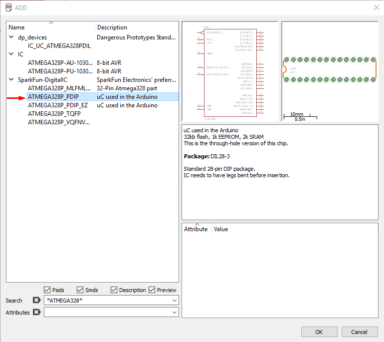
If that component doesn’t show up in the search, try following the library install process as shown in the tutorial linked above. Now place it on the schematic sheet. The best thing to do is to get all the components you need, lay them out on the schematic sheet roughly where you want them, then start connecting everything up with nets.
Now, using the complete reference schematic attached, open it up in a separate Eagle window, and right click on eagle schematic symbol and click properties. This will bring up the component info, look for the Device name, and put either part, or all of it in the Add component search, and add each component as we did with the Atmega328. Bring all the components into your schematic sheet, laid out similarly to the reference.

Awesome sauce, by now your schematic should look a little something like this:

As you can see in the image, you can see that some of the components such as the resistors and capacitors have values for the resistance and capacitance. To give a component a value, use the Value tool, click on the component, and enter it in there.

The components are laid out roughly where they need to go, nicely spaced out, with the appropriate values, but there is nothing connecting them, so let’s connect up all of our nets for the components, but rather than going through and connecting up our power and ground lines, we’ll use symbols to attach to the end which will automatically connect them electrically, but keep everything looking clean. When we want to connect components together, we use what is called a ‘net’. You can connect any number of components to a net, and they don’t have to be literally connected, if you right click on the properties for that net, you can change the name, and nets that have the same name will be connected when we move to the PCB design. To create a new net, click on the net tool, and draw them in.

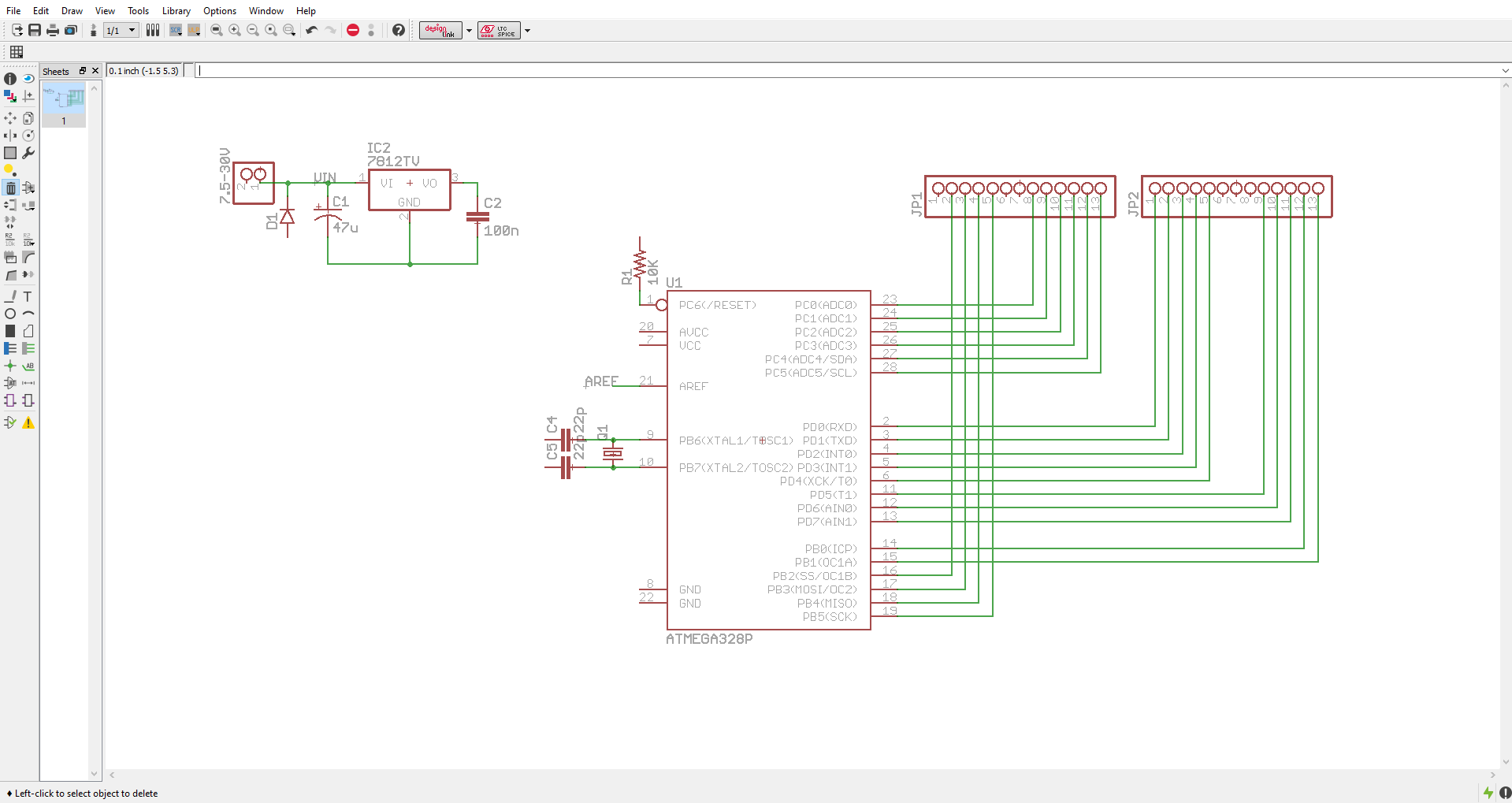
It’s looking more and more like a complete circuit now, but as mentioned above, there is no power connections or ground connections. For this, we need to go back to the Add component tool, and scroll down through the libraries until we get to Supply 1 and Supply 2. These libraries contain these power symbols. Which library you use is up to your visual preference, and what options they have. Go in and add GND (ground) and VCC/power symbols where shown on the reference schematic.
Something else you’ll notice about the reference schematic are the labels on some nets which I used to connect different points of the schematic to each other to keep everything nice and clean. To do this, use the Label tool, click on the net, and place the label. As mentioned before, to connect different nets together, you can right click and go into properties to make the net names the same, or you can use the Name tool.

Fantastic, everything is connected up, labelled, and well laid out. Our schematic is complete! At this point, a wise person would go through and check connections, make sure that all of the pin labels and details are correct.

There you have it, a schematic, you created from scratch, which contains stacks of information, and we can now use to create a professional PCB, ready for product.
What Now?
Schematic creation is only the first step of our Eagle tutorials, to turn our schematic into a PCB layout, move on to our PCB Design With Eagle tutorial.

